If you haven’t already, I suggest you check out my about page. It might save you from reading this if you’re looking for an authoritative view of the world.
I don’t care how hard the likes of Nvidia try; microchips, or “semiconductors” as the establishment calls them, aren’t sexy. That’s not to say they aren’t beautiful though. This ode to semiconductor precision in Simon Winchester’s Exactly makes a good case for them:
The technology… is performed on such an infinitesimally minute scale, and to tolerances that would have seemed unimaginably absurd and well-nigh unachievable only decades ago, that it is taking precision into the world of the barely believable — except that it is a world that manifestly must be believed, a world from which, one can argue, modern humankind benefits mightily and for whose existence it is all the better…
I think of “semis” as the key workers of the Information Age, out of sight to most of us as technology consumers but reliably serving our excessive computational demands. And last year, as with every passing year, felt like compute’s biggest order yet: GPT-3 plagued Twitter, SpaceX launched astronauts to the ISS, and DeepMind’s AlphaFold solved the greatest challenge most of us had never heard of before.
These headlines don’t happen without the semiconductor industry.
Maybe at odds with my key worker analogy, it did receive a generous share of credit in the markets; Nvidia breached $300bn in market cap for example. This number didn’t mean much to me initially, but I then realised it implies, albeit in the loosest sense maybe ever, that Nvidia’s more valuable than household names like Nike and Coca-Cola.
I started to explore semis in November when Apple’s latest MacBook was released with its new chip inside. It was the talk of techie town, but I didn’t understand what the fuss was all about. After just a bit of digging around though, I was kicking myself for previously dismissing the world of chips for gamers with a hardware fetish.
The significance of the semiconductor industry isn’t particularly difficult to grasp; it sets the pace for most of the world’s computational-based innovation. The outcomes of this responsibility transcend just hard science though. The industry pioneered the now-ubiquitous “make it up in volume” dogma of “tech economics”, as Ben Thompson calls it. It’s also at the forefront of geopolitics and foreign policy.
The semis ecosystem is dominated by a handful of companies playing at the boundaries of physics and protecting their discoveries with security measures comparable to the most paranoid of nation states. There’s something fascinating about this concentration of value; if an earthquake hit any one of these companies, the shock waves would propagate destruction throughout the global data economy.
All that to say, I was always going to kick this blog off with semis; I don’t care how overcrowded the writers’ bandwagon is.
The ecosystem
The semis value chain looks something like below.
The model above isn’t complete; I’m missing semis like analog and mixed-signal devices. It’s also probably not entirely valid; I don’t know much about FPGAs so I just stuck them in their own subset of chips for example. Anyway, I think it captures most of the important relationships and I’m going to explain them over the next few posts. Also, I’ll update it if I learn something new (as with everything I write).
In this post, I’m focusing on foundries that fabricate logic and system semiconductors. This basically means more processor, i.e. execution, and less memory, i.e. storage.
A disgracefully abstract technical primer
As always, I had to figure out where the foundries sit in the technical stack before I started to explore the market. If this stuff brings back bad memories, feel free to skip to the next section that’s more market focused.
It turns out foundries literally fabricate computers into physical reality; not the screen, shiny metal casing, or that type of interface for you to interact with them, but the chips that actually perform the computation using electronic circuits directing flows of current meaningfully.
The type of electronic circuits found in most computers are “integrated circuits”, which is why that term is synonymous with chips. I’d always thought that the “integrated”part referred to some abstract functional integration, but it’s actually straightforwardly physical. Fundamental electronic components of the circuits are “printed” directly into a wafer of silicon. This works because silicon is inherently semiconducting, which means current can flow through it under certain conditions.
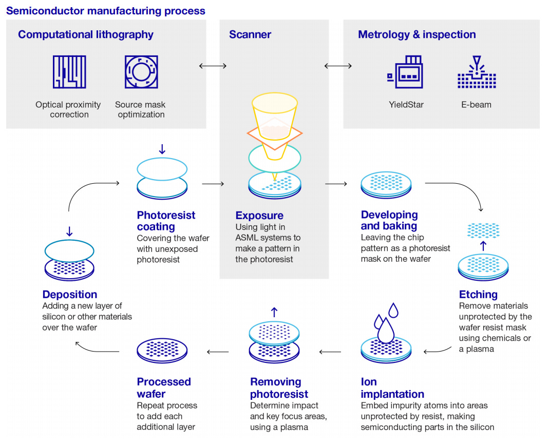
To say “printed” is simplistic, but it conveys the fact that these components are built into the silicon wafer, similarly to ink on paper. An important part of the process involves optical lithography (i.e “printing” with light), but there are several other parts as you can see below.
One of the fundamental electronic devices that are fabricated during this process are transistors. Transistors can be simply thought of as binary switches, which have an “on” or “off” state, encoding 1 “bit” of information by the measure’s definition.
The “on” state is defined as when a positive voltage is applied across the transistor’s “gate” (peep the image below), which creates an electric field that allows electrons to flow from the source to the drain through the silicon wafer. The “off” state is just when nothing’s flowing.
Transistors can be wired together, and with other fundamental electronic devices, using “interconnects”. These form logic gates that physically implement logical operations with binary input and output.
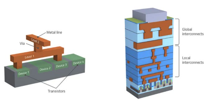
So, we can compute any logical operation we want to. There it is… a computer.
I’ve conspicuously avoided many complex chains of abstraction that take us to a representative model of a normal computer that people actually use. I haven’t even mentioned anything about memory for example. But, I won’t pretend to know much more.
In terms of what the final product of the foundries looks like, the disk in Francis’ hands below is not too far off. It’s a bunch of shiny integrated circuits packed into a silicon wafer (usually 30cm wide), which is then sent off to assemblers who cut out the individual chips and package them into the small black pieces that get put up for retail.

The number of transistors being used in each of these integrated circuits has been exponentially increasing since their commercialisation in 1971.
Gordon Moore is partly to blame for this trend. In 1965, he declared that transistors, among other fundamental electronic devices, would halve in size every year. This was later amended to every two years, and chipmakers seemingly desperate to adhere to the Godfather’s prescription have roughly been achieving this.
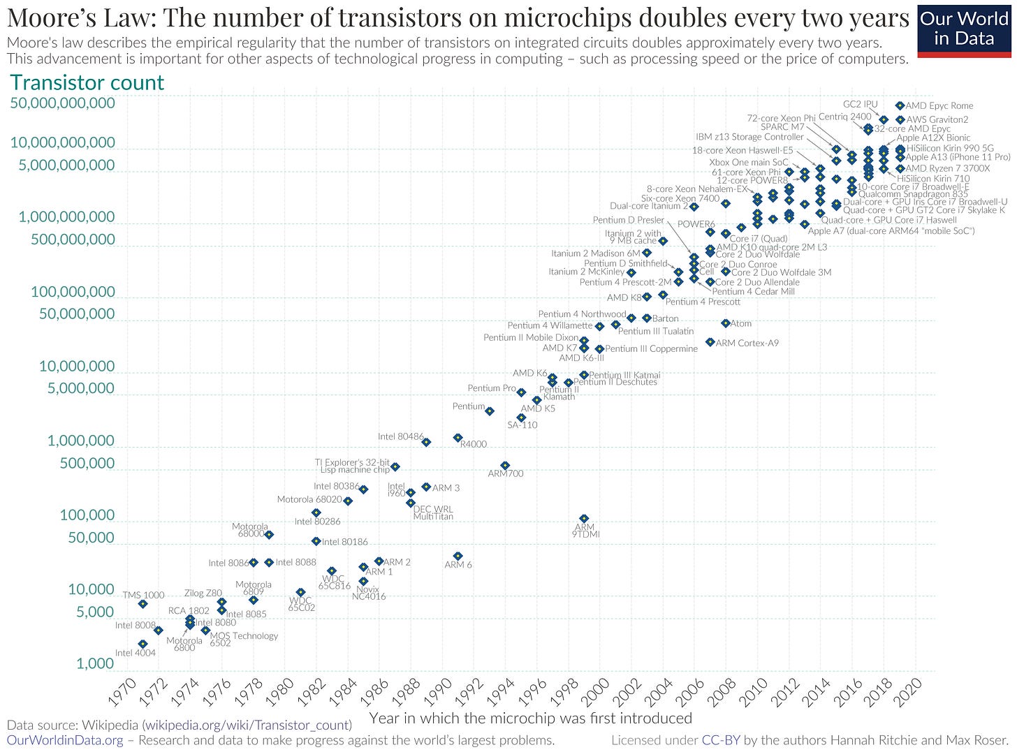
The consensus is that this trend explains, in part, why chips have been getting more powerful since their commercialisation. The explanation is more controversial than I thought it would be, but it seems that smaller transistors basically mean that more circuits can be fitted onto a single piece of silicon, enabling more computational parallelism, and that each transistor requires less power, and so can be turned on and off more quickly to encode information.
There’s talk about being at the end of “Moore’s Law” because we’ve reached the physical limits of a transistor; they’re about 10,000 times thinner than a human hair in the new MacBook. I’ve encountered futurists using this to claim that binary computing is Boomer technology and it’s quantum’s time to shine.
Unfortunately for that likely Zoomer, innovation in heterogeneous compute, domain specific architectures, 3D packaging, and other witchcrafts mean that Shannon’s bits are still it for the near future. I’ll dive into that stuff when I’m done with the basics.
There’s an overwhelming amount of stuff out there on semis, but I’ll highlight some of my favourites. There are some excellent primers in Mule’s Musings.

I enjoyed this introduction to the fabrication of a chip. It’s from 2012, which is ancient in semiconductor time, but it covers most of the fancy words I used to kid myself about understanding. By the way, I’ve set that link to start playing with a hilarious clip of a foundry fail that you should watch even if you’re not interested in the whole video.
Also, James Gleik’s The Information is a brilliant history of information and computation as concepts; I can’t recommend it highly enough. It’s for people with or without a technical background.
Anyway, onto the market.
TSMC and its impregnable moat
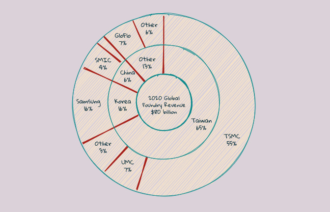
It didn’t take long for me to realise that there’s one runaway leader in the foundry game: Taiwan Semiconductor Manufacturing Company (TSMC).
This quote from Mule sums up the company’s influence:
TSMC is like the sun, and all the world’s semiconductor companies orbit around it. Whether if you compete against it (Samsung, Intel, Global Foundries), or you are reliant on it (everyone), what TSMC says and does matters.
I recommend this interview with Morris Chang, TSMC’s founder, who goes through the company’s origin with better storytelling than mine, but I’ll go over it anyway.
TSMC is the oldest pure-play foundry; it fabricates chips but doesn’t design its own. When it entered the semiconductor industry in 1987, TSMC struggled as its only business was the leftovers of vertically integrated manufacturers (IDMs) that designed and fabricated its own chips.
The concept of being a “fabless” chip designer (without its own foundry) didn’t exist before TSMC. Jerry Sanders, CEO of one those IDMs, once said “real men have fabs”. To the dismay of Jerry’s masculinity, technologists realised with TSMC that they could outsource chip fabrication and avoid its toxic costs. The fabless design ecosystem then mushroomed, and TSMC reaped the benefits of a first-mover advantage in a game where cumulative knowledge trumps all.
After seeing it mentioned a lot in the past few months, I felt obliged to read Clay Christensen’s The Innovator’s Dilemma. I’ve only flicked through, but his insights seem to hold out well for the TSMC story.
Perhaps the most powerful protection that small entrant firms enjoy as they build the emerging markets for disruptive technologies is that they are doing something that it simply does not make sense for the established leaders to do. Despite their endowments in technology, brand names, manufacturing prowess, management experience, distribution muscle, and just plain cash, successful companies populated by good managers have a genuinely hard time doing what does not fit into their model for how to make money. Because disruptive technologies rarely make sense during the years when investing in them is most important, conventional managerial wisdom at established firms constitutes an entry and mobility barrier that entrepreneurs and investors can bank on. It is powerful and pervasive.
TSMC receive significant backing from the Taiwanese government. But, credit where credit’s due, it resourcefully invested into manufacturing excellence, led the way in patent application, and established deep relationships with the best designers. All are testament to TSMC’s technical and strategic competence.
The analysis of TSMC’s strategy in this conversation with Jay Goldberg is insightful. I particularly enjoyed the discussion of a “pendulum of integration” that describes the trade-off in benefits between the cost aggregation that comes with modularisation and the functional optimisation with vertical integration. TSMC is the poster child for the modularity end of this pendulum.
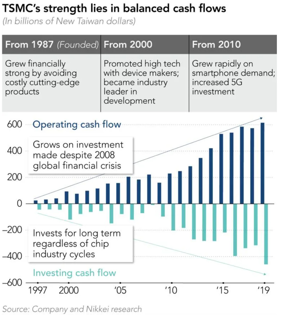
What’s clear from all the analysts is that TSMC has dug a moat as deep as they come. And it’ll continue to be reinforced as the company builds barriers of capital expenditure that are intimidating for any risk-averse competitor. A state of the art lithography machine costs about $120mn a pop and TSMC claims to own over half of the them, spending $19bn on capital last year (roughly the same as the other foundries combined).
A start-up would probably need about $30bn up front to even think about being competitive, and that doesn’t consider the time that’s then required to catch up with TSMC in terms of process knowledge. The importance of tacit knowledge in foundries is highlighted in this conversation with Willy Shih.
The costs in the chart below seem deflated compared to what I’ve heard, but it still depicts how drastic they are for foundries and how they get worse as the foundries fabricate “smaller” chips.
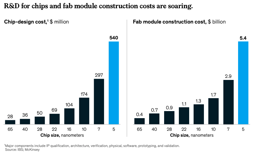
“Chip size” on the horizontal axis actually refers to the “process node” used for chip fabrication, which is a term coined by the foundries to market each generation of their process technology. It still sort of confuses me, but a process node doesn’t have much to do with a size that can be measured with some microscopic ruler; it just uses the “nm” suffix and represents an improved process with a smaller number. That is, a 5nm process process generally produces more powerful and efficient chips than a 7nm process node. The “nm” suffix is a legacy of a pre-2000s trend where the number was synchronised with the transistors’ gate length. When this trend broke down, foundries just decided to stick with convention to market a new generation.
There’s more to a better process than smaller transistors: the type of transistor implemented, the proportion of chips etched into the silicon wafer that aren’t defective (i.e. the yield), and many other variables are important for generational classification.
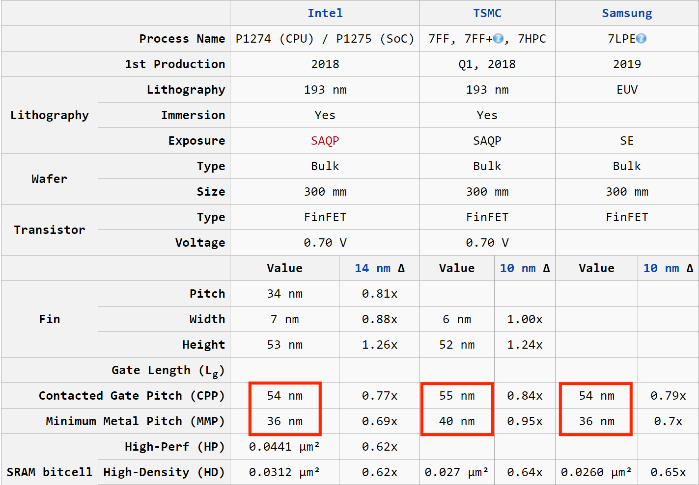
It’s fair to say that standardisation of the contemporary metric isn’t the clearest. For example, people claim that Intel’s 10nm process is equivalent to TSMC and Samsung’s 7nm. However, apparently there’s still enough substance in the measure to say something like “foundry X is a N generations behind foundry Y”. This article explains what’s going on in more detail.
The hype in November around Apple’s new chip was partly around its use of TSMC’s 5nm process. Apple had been buying off-the-shelf central processing units (CPUs) and graphical processing units (GPUs) from Intel since 2006 with the release of the first MacBook Pro. Despite owning my MacBook for years, I never considered the importance of the Intel gear inside it — probably because it doesn’t have that naff “Intel Inside” sticker on it that I’m sure was great marketing once upon a time. Regardless, Apple cutting ties with Intel for its Macs and designing it own chips using TSMC was a big moment in semis history.
Apparently the move actually wasn’t much of a surprise for those in the know. Apple has been designing its own chips for the iPhone, the A-series, since 2010 and have been using TSMC for fabrication since the A8 in 2014. It goes without saying that its custom silicon has been successful for the iPhone, so doing the same for the Mac was arguably inevitable. Apple is now TSMC’s largest customer, probably accounting for about 20% of TSMC’s $45bn in yearly sales


2020 wasn’t flawless for TSMC though.
The US Department of Commerce added Huawei to its “Entity List”. This means that no one using above a “25% threshold of US technology” in its manufacturing process can sell to China’s largest smartphone manufacturer without a license that’s difficult to obtain.

I’m not exactly sure how TSMC’s fabrication process breaches the threshold. I think it’s something to do with the lithography machines it uses. There’s only one global supplier for the state of the art and they do use US technology, so it would make sense why TSMC can’t just switch it up (as well as geopolitical reasons). I’ll dive into capital equipment at some point (…I’m making too many promises).
Most count this as a blow for TSMC because it had to shut up shop to Huawei in September despite accounting for about 15% of TSMC’s sales at the start of 2020, up from 5% a couple years before.
And Tim Culpan highlights why this geopolitical problem for TSMC may not go away if the Sino-American relationship worsens. TSMC probably wouldn’t be able to continue with its neutral stance between the two, and the most likely outcome would be it siding with the US. It’s more American in its culture than it’s Chinese despite geography; the two men to have ever run TSMC are both US citizens, it’s poached former Intel employees for lobbying, and it's planning to pump $10bn into a new fab in Arizona this decade. Signs of a closer relationship with China are apparently not there.
I guess we’ll have to see what happens; that’s bigger than semiconductors. For now, pretty much every device in every country, from your phone to the nearest traffic light, will have TSMC inside.
Samsung’s efforts to muscle in
I must admit that I didn’t realise how much more Samsung produces than phones I’ve never really given a look-in. It runs a foundry within its electronics department that fabs its own chips (e.g. in its Galaxy smartphones) as well as the chips of external designers. I think a large portion of its revenue comes from external customers, although I haven’t found a credible stat on this.
Samsung is the only other foundry just about keeping up with TSMC in terms of the bleeding edge; it’s the only other with a 5nm process. Saying that, its sales were about a third of TSMC’s last year at $15bn (I had to do some inference from their earnings report for that, so I apologise if its inaccurate).
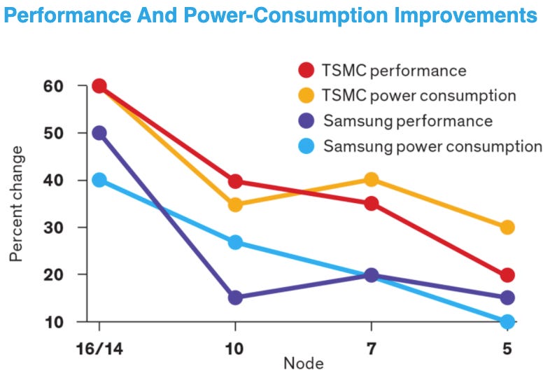
Samsung announced in its clichéd “Vision 2030” that it wants to overtake TSMC in semis this decade, planning to invest around $120bn. A punt for some return on that is its transition from fin field-effect transistors (FinFET) to gate-all-around transistors (GAAFET) in its upcoming 3nm process, already delayed for a year but expected to be commercialised in 2022. The move precedes TSMC’s transition to GAA for 2nm in 2024.
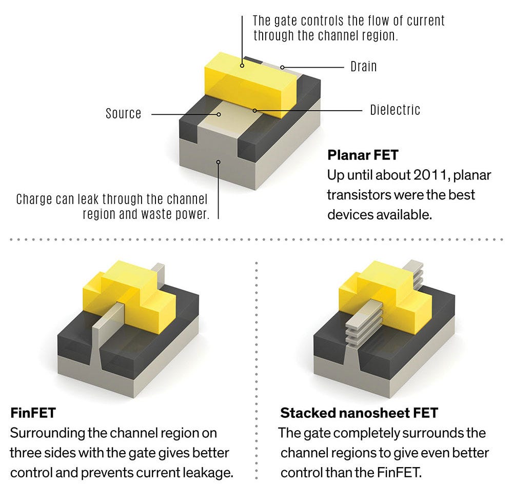
Despite Samsung’s flashy promo, its move doesn’t seem enough to justify a drastic bear case for TSMC who claims to have improvements left in FinFET. Also, having locked in contracts for 5nm with most leading chip designers and Apple for 3nm (with mass production for 2022), it makes sense why TSMC aren’t in too much of a rush to tinker with their transistors.
It took me longer than it should’ve to realise the importance of contracts in the foundry game. Apple began testing TSMC’s 5nm process in October 2019 for the A14 chip in the iPhone 12, which then wasn’t being sold in Apple stores until a whole year later. So, I presume for all that time in contract TSMC had secured Apple’s rather large bag.
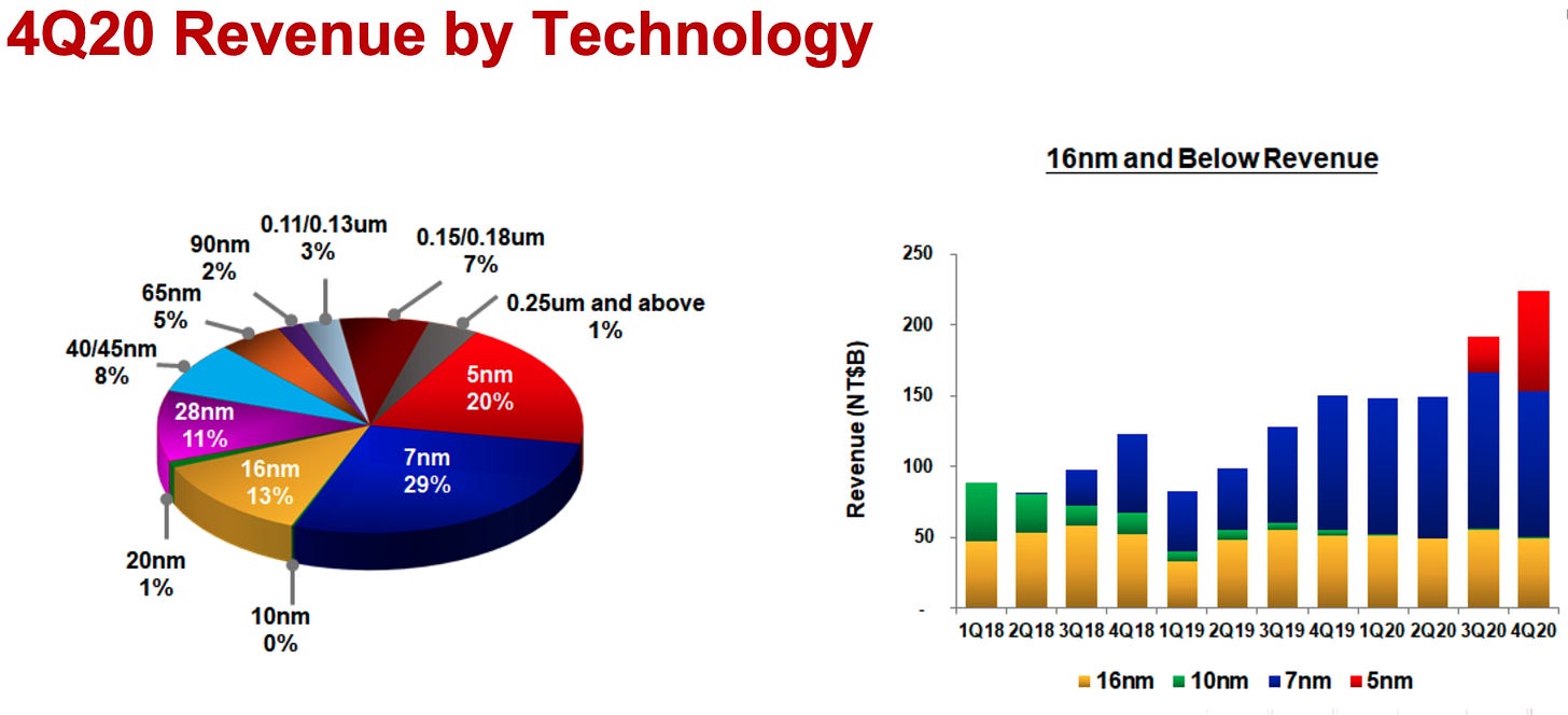
Also, not every fabless chip designer might want Samsung’s fancy transistors. I don’t have the equivalent data for Samsung, but 29% of TSMC’s revenues in 4Q20 came from 7nm and 13% came from 16nm despite being commercialised years ago. Sometimes the bleeding edge is just unnecessarily expensive for certain applications as well as less reliable in terms of yield, time to market, and design support. This conversation with Tom Caulfield sheds some light on the significant market for “larger” process nodes.
To get some perspective on the process node race, I’ve plotted out the timeline below. I’ve tried to normalise the number according to industry standards, but it’s all a bit noisy so forgive me for any inaccuracy!
You can see Samsung and TSMC are pretty much neck and neck. As for who’s going to be on top in 2030, I don’t believe anyone who confidently claims to know the answer.
China’s struggle to dig its own
I’m just another Sinophile that ignorantly romanticises “Chinese Tech”, so of course the last part of the foundries ecosystem I’m going to gloss over is China.

I’m certainly guilty of reading an anecdotal story about some technical feat in China and concluding it’s a land of flying cars and holograms. This conversation with Dan Wang paints a less naive picture of the Chinese landscape.
Either way, China’s appetite for semis is uncontroversially large. It consumed almost 60% of the world’s global supply of semis last year. And in a bid to win the tech race the world seems to be in, Beijing has pledged just under $2tn through 2030 for investment into technology such as cloud computing centres and 5G base stations.
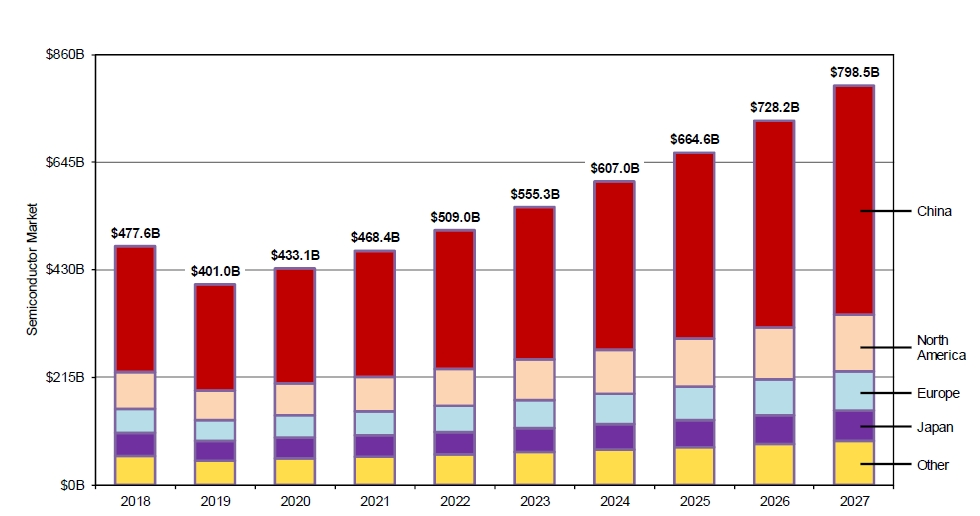
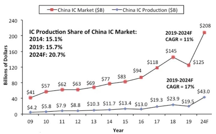
There’s no doubt Beijing’s stimulus will build up the Chinese appetite for compute, but the CCP are keen for this to be home fed. The 14th Five-Year Plan and Made in China 2025 are all about securing technological autonomy. This means reducing imports and closing the production-consumption gap; the goal for semis is to produce 70% of all consumption by 2025.
The data I’ve found about Chinese semis seems quite noisy. This paper suggests China’s production share of the market was just under 10% in 2018, whereas the chart below suggests its was just over 15%. Still, the point remains that 70% in just a few years seems very ambitious.
Naturally, a large part of Beijing’s plan involves pouring a load of money over the problem. For example, the state-backed National Integrated Circuit Investment Fund raised $29bn in 2019. Of course, the “official” Crunchbase logs are sparse but you can see that the fund pumped $2.3bn of that last year into China’s leading foundry, Semiconductor Manufacturing International (SMIC).
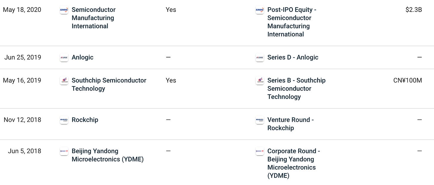
However, the consensus seems to be that money won’t solve all of China’s infancy problems in semis fabrication anytime soon. While it’ll help in terms of capital expenditure and wooing engineers with fat compensation packages, it won’t in accumulating the tacit process knowledge that’s required to run a leading foundry.
Fabricating semiconductors is apparently just incredibly difficult. Even with all the right machinery, knowing how to turn all the knobs correctly is hard. This nod to compound interest from Willy Shih sheds some light:
If 99.99% of the chips passing through a single step are free of defects, by the time you make it through 700 steps only 50% of the individual chips will be good. This is after carrying them through a two month production process. Thus manufacturing process control is paramount: dipping to 99% yield for each step would result in zero yield overall.
700 steps is apparently typical for a fabrication process, and foundries have to master each and every one. So unfortunately for SMIC, unless Beijing hijack TSMC’s whole workforce as well as the long-standing Taiwanese ecosystem around the company, it’ll continue to be about 10 years behind in terms of the bleeding edge for a while. And no, an invasion isn’t really on the cards; China would be sanctioned to the ground.
That is, sanctioned even more than it already is. SMIC was put on the Entity List alongside Huawei. I didn’t find any other Chinese foundries in the list, but I probably wasn’t looking hard enough (it’s a long and convoluted document). As a side note, whatever this means, I did a ctrl-F in the PDF with ‘China’ and it matched 705 times; ‘Iran’ matched 144 times.
The chart below is a rather consultant way of showing these supply concerns for China.
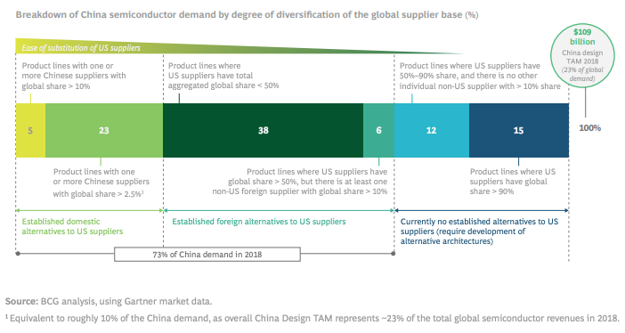
It seems like a pretty sticky one for SMIC and other Chinese foundries. I haven’t come across much analysis on how they’re going to overcome this, but one claim made by Willy is that 10, 20, 50 years isn’t a long time for Beijing. At least, it’s not as long as it is to Washington; an average Chinese dynasty is about as long as the whole of US history. This idea of Chinese “long term orientation” might just be a stereotype, but I did find some cited papers on the claim.
Also, and this is pseudo-analysis at best, Beijing generally seem to know how to mobilise its country out of crises. Its ruthless handle of Covid highlighted this for me, so I’m not going to just blow off China in semis.
For another time
I’ve left out a few major foundries. UMC and GlobalFoundries have both dropped out of the bleeding-edge race and produce “specialty” chips, which don’t excite me so much. This is silly of me because they’re both still important players in the ecosystem. In fact, I just found out (again frustratingly late) in this conversation with Jeremy O’Brien that semiconductors are tightly coupled with the “photonics” approach to quantum computing and that GloFo are making some movements in the space.
I’m also saving Intel for another post because its story, which I touched on with the Apple stuff earlier, is very juicy. It commercialised the first microprocessor ever and has since been a stalwart of semis. The consensus is that Intel grew complacent and then flopped with the smartphone opportunity. A few more blunders since and the bears are claiming that Intel’s now in the mud.
Thanks for reading this . Feel free to comment any corrections or general thoughts.
Share this article with your friends if you enjoyed it!
Subscribe to keep up to date.
And connect with me on Twitter if you’re interested in following my general musings.


This was amazing.
hey man! Great stuff this is a great post. I really really appreciate the shoutouts :D Cheers - seems like you got a good handle on things.